How to Design an Effective PCB Layer Stack-Up
A well-designed PCB Layer Stack Up forms the backbone of any electronic device. The arrangement of copper and insulator layers influences the electrical performance significantly. A precise stack-up enhances signal integrity and reduces electromagnetic interference. Engineers must prioritize this aspect to ensure optimal functionality. A robust stack-up design also contributes to the reliability of the circuit over time. Proper layer arrangement minimizes potential issues, ensuring long-term stability. The importance of a strategic PCB Layer Stack Up cannot be overstated in achieving high-quality electronic products.
Fundamental Concepts of PCB Layer Stack-Up
Arrangement of Copper and Insulator Layers
Role of Copper Layers
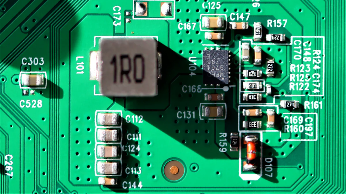
Copper layers in a PCB Layer Stack Up play a crucial role in conducting electrical signals. Engineers use copper layers to create paths for current flow. Copper conductors have inherent DC resistance, which helps dissipate heat. This characteristic enhances the thermal management of PCBs. Effective heat dissipation prevents overheating and ensures the longevity of electronic components. Copper layers also contribute to signal integrity by reducing electromagnetic interference.
Role of Insulator Layers
Insulator layers separate the conductive copper layers in a PCB Layer Stack Up. Dielectric materials provide this insulation. Proper selection of dielectric materials prevents faulty signals from affecting circuit performance. Insulator layers maintain the structural integrity of the PCB. The design of these layers influences the overall insulation characteristics. External factors and the electric field form also impact insulation performance. Engineers must consider these aspects when designing PCBs.
Role of Power and Ground Planes
Importance of Power Planes
Power planes distribute power evenly across the PCB. These planes ensure that each component receives the necessary voltage. A well-designed power plane reduces voltage drop and power loss. Power planes also enhance thermal management by spreading heat. This distribution helps maintain optimal operating temperatures. Engineers prioritize power plane design to achieve efficient power delivery.
Importance of Ground Planes
Ground planes provide a reference point for all electrical signals. These planes help minimize noise and electromagnetic interference. Ground planes also improve signal integrity by providing a return path for current. Keeping power and ground layers together enhances performance. This arrangement reduces potential issues with crosstalk and signal distortion. Engineers must carefully design ground planes for effective PCB Layer Stack Up.
Specific Design Considerations for PCB Layer Stack Up
Maintaining Minimum Distances
Between Power and Ground Planes
Maintaining a minimum distance between power and ground planes is crucial. Engineers must ensure that these planes are close enough to reduce inductance. Reduced inductance enhances the performance of the PCB Layer Stack Up. A closer proximity between power and ground planes also improves signal integrity. Engineers achieve better voltage regulation by minimizing this distance.
Between Signal Layers
Signal layers require careful spacing to prevent interference. Engineers must maintain a minimum distance between signal layers to avoid crosstalk. Crosstalk can degrade the quality of signals in a PCB Layer Stack Up. Proper spacing ensures that signals remain clear and distinct. Engineers must calculate the optimal distance based on the specific design requirements.
Avoiding Adjacent Signal Layers
Reasons for Avoidance
Adjacent signal layers can lead to significant issues. Engineers avoid placing signal layers next to each other to minimize crosstalk. Crosstalk occurs when signals interfere with one another. This interference can cause data errors and reduce the reliability of the PCB Layer Stack Up. Engineers prioritize the separation of signal layers to maintain signal clarity.
Alternative Arrangements
Engineers use alternative arrangements to prevent adjacent signal layers. One common method involves placing a ground plane between signal layers. This arrangement reduces the risk of crosstalk. Another approach involves staggering the signal layers within the PCB Layer Stack Up. Staggering helps maintain the integrity of each signal path.
Ensuring a Symmetric Stack-Up
Benefits of Symmetry
Symmetry in a PCB Layer Stack Up provides numerous benefits. A symmetric stack-up ensures balanced mechanical properties. Balanced properties prevent warping and bending during manufacturing. Symmetry also contributes to consistent electrical performance. Engineers achieve uniform impedance across the PCB by maintaining symmetry.
Techniques for Achieving Symmetry
Engineers employ specific techniques to achieve symmetry. One technique involves mirroring the layer arrangement from the center outward. Mirroring creates a balanced structure in the PCB Layer Stack Up. Another technique includes using identical materials for corresponding layers. Identical materials ensure uniform thermal expansion and contraction.
Technical Demands of the PCB Layer Stack Up
Controlled Impedance
Definition and Importance
Controlled impedance is essential for maintaining signal integrity in high-speed PCB designs. Engineers must manage the electrical characteristics of traces to ensure consistent signal flow. Impedance mismatches can cause signal reflections, leading to data errors. High-speed applications require precise impedance control to prevent these issues. The design process involves calculating trace widths and spacing to achieve desired impedance levels.
Methods to Achieve Controlled Impedance
Designers use specific techniques to maintain controlled impedance. Calculating and maintaining consistent trace widths is crucial. Differential pair routing helps manage impedance for high-speed signals. Engineers use impedance calculating software to determine wiring parameters. These parameters guide the PCB layout and wiring process. After manufacturing, an impedance test verifies the accuracy of the design.
Crosstalk Control
Causes of Crosstalk
Crosstalk occurs when signals on adjacent layers interfere with each other. This interference results from electromagnetic coupling between traces. High-speed signals are particularly susceptible to crosstalk. Engineers must address this issue to maintain signal clarity. Crosstalk can degrade performance and lead to data errors.
Strategies for Minimizing Crosstalk
Engineers employ several strategies to minimize crosstalk. Increasing the distance between signal layers reduces electromagnetic coupling. Placing ground planes between signal layers provides additional isolation. Staggering signal layers within the stack-up also helps. These techniques ensure that signals remain distinct and clear.
Interplane Capacitance
Understanding Interplane Capacitance
Interplane capacitance refers to the capacitance between power and ground planes. This capacitance affects the electrical characteristics of the PCB. Engineers must consider interplane capacitance when designing high-speed circuits. Proper management of this capacitance enhances signal integrity.
Impact on Signal Integrity
Interplane capacitance plays a significant role in signal integrity. High interplane capacitance can lead to unwanted signal coupling. Engineers must balance capacitance levels to maintain performance. Properly designed interplane capacitance improves power distribution and reduces noise. This balance ensures reliable operation of high-speed circuits.
Material Selection and Signal Layer Estimation
Choosing the Right Materials
Factors to Consider
Selecting the appropriate materials for a PCB involves evaluating several critical factors. Engineers must consider the dielectric constant of materials, which affects signal integrity and performance. Thermal properties play a significant role in determining how well a PCB can handle heat dissipation. The choice of materials impacts the electrical characteristics and safety of electronic devices. Engineers must also assess the quality of copper foil and dielectrics to ensure reliable signal transmission. Proper material selection minimizes attenuation and enhances the overall performance of the PCB.
Commonly Used Materials
Several materials are commonly used in PCB manufacturing due to their favorable properties. FR-4 is a popular choice because of its balance between cost and performance. This material offers good thermal and electrical insulation properties. Polyimide is another option that provides excellent thermal stability, making it suitable for high-temperature applications. Rogers materials are often used in high-frequency circuits due to their low dielectric loss. Engineers select materials based on the specific requirements of the application, ensuring optimal functionality and durability.
Estimating the Number of Signal Layers
Criteria for Estimation
Determining the number of signal layers in a PCB involves careful consideration of design complexity and circuit requirements. Engineers evaluate the size and intricacy of the circuit to decide the necessary layer count. Higher layer-count stack-ups may be required for complex designs with multiple signal paths. The decision also depends on the need for controlled impedance and crosstalk control. Engineers must balance these technical demands with the available space and budget constraints.
Balancing Performance and Cost
Achieving an effective balance between performance and cost is crucial in PCB design. Engineers strive to optimize the number of signal layers to meet performance goals without exceeding budget limits. A higher number of layers can improve electrical performance by providing more routing options and reducing interference. However, additional layers increase manufacturing costs. Engineers must carefully assess the trade-offs to design a cost-effective PCB that meets performance standards.
For optimal electrical performance, prioritize maintaining minimum distances between power and ground planes. Avoid placing signal layers adjacent to each other to minimize crosstalk. Use symmetric stack-ups for balanced mechanical properties. For complex designs, consider higher layer-count stack-ups to accommodate intricate circuits. Choose materials like FR-4 or polyimide based on thermal and electrical needs. Engage with the design community by sharing experiences and seeking feedback. Continuous learning and adaptation will enhance your PCB design skills.